
When do graphene materials improve display electrode performance?


When Do Graphene Materials Improve Display Electrode Performance?
Graphene Materials for displays become relevant when a conventional transparent electrode is no longer meeting the real engineering constraints of the product. That usually means the issue is not simply conductivity. A display developer may be dealing with repeated bending, a curved cover stack, a brittle indium tin oxide (ITO) layer, an electrode that cracks after lamination, or a process route that cannot tolerate high-temperature deposition and annealing.
For technical evaluators, graphene is not a universal replacement for ITO. In many rigid flat-panel applications, ITO remains difficult to displace because the manufacturing ecosystem is mature, its optical behavior is well understood, and its integration rules are familiar. Graphene earns consideration when its particular combination of flexibility, thinness, chemical stability, and potentially low-temperature compatibility solves a problem that ITO, metal meshes, conductive polymers, or oxide alternatives do not solve cleanly.
The practical question is therefore narrower: under what operating and manufacturing conditions can a graphene-based transparent conductor improve electrode performance without creating larger problems in uniformity, contact engineering, patterning, or yield?
The first distinction: “graphene” does not describe one electrode material
A screening program can go wrong before electrical testing starts if all graphene offers are treated as equivalent. Large-area chemical vapor deposition (CVD) graphene, reduced graphene oxide (rGO), liquid-phase exfoliated graphene, graphene nanoplatelet inks, and graphene-containing hybrid coatings have very different transport paths, optical losses, surface textures, and production risks.
CVD graphene can form a highly thin, continuous conductive film with strong optical transmission. It is often the most relevant form for transparent electrodes in demanding flexible OLED, touch, or specialty optical-stack work. Its challenge is not the concept of conductivity; it is achieving repeatable transfer, low contamination, controlled multilayer regions, and stable electrical contact over panel-scale areas. Grain boundaries, wrinkles, cracks introduced during transfer, and residues from support layers can dominate finished-film performance.
Solution-processed graphene materials are attractive where coating cost, substrate size, printing compatibility, or low-temperature processing matter. Yet an ink-based film conducts through a network of overlapping flakes rather than through a single continuous atomic layer. The junction resistance between flakes, binder selection, drying profile, surface roughness, and post-treatment all affect the result. Such materials may suit selected touch sensors, transparent heaters, antistatic layers, or less demanding electrodes, but they should not be assumed to match the optical and electrical behavior of high-quality CVD graphene.
That distinction should be written directly into the evaluation plan. A supplier’s use of the word “graphene” is not enough to define a comparable bill of materials.
Where graphene has the clearest performance case
The strongest application case is usually mechanical rather than purely electrical. ITO performs well on rigid glass, but it is brittle under tensile strain. Once a display architecture introduces repeated flexing, folding, rolling, local curvature, or deformation around a small radius, cracking in the transparent electrode can increase resistance and create visible non-uniformity. A properly integrated graphene film can remain conductive through deformation modes that are inherently difficult for a brittle oxide layer.
This does not mean a graphene electrode automatically survives a flexible display qualification. The full stack still matters: substrate modulus, encapsulation, adhesive behavior, neutral-plane placement, patterned metal traces, and the interface between graphene and busbars can all become the first failure location. But if electrode cracking is the limiting mode, graphene deserves a serious comparison rather than being treated as a laboratory curiosity.
Graphene can also be useful where extreme thinness has optical or mechanical value. A very thin conductive layer can reduce the thickness burden in compact optical stacks and may avoid some of the fracture and texture concerns associated with thicker coatings. For transparent devices, however, “thin” is not the same as “invisible.” The relevant evaluation includes transmission across the display’s operating spectral range, haze, reflected appearance, color shift, and interaction with polarizers, anti-reflection coatings, and adhesive layers.
Another realistic use case is a hybrid electrode. Graphene may be paired with a fine metal grid, conductive polymer, carbon-based coating, or another transparent conductor to balance sheet resistance and transmission. Hybrid designs can be more practical than asking graphene alone to carry current across a large active area. They also introduce new issues: grid visibility, galvanic behavior, layer-to-layer adhesion, pattern registration, and local current crowding at contacts.
Sheet resistance is necessary, but it is not the decision
Most graphene electrode discussions begin with sheet resistance. They should begin there, but not end there. A sheet-resistance value measured on a small coupon can look promising while the finished display shows edge darkening, voltage drop, non-uniform touch response, or unstable pixel driving. The gap between coupon performance and module performance is often caused by contact resistance, film continuity, and spatial variation.
For a display electrode, the useful measurement set depends on the application, but the following questions are hard to avoid:
- What is the sheet-resistance distribution across the actual usable panel area, not only at a central test point?
- At the required optical transmission, how much haze or visual texture does the film introduce?
- How stable is resistance after bending, thermal exposure, humidity exposure, lamination, and handling?
- What is the contact resistance to the chosen metal busbar or interconnect stack?
- Can the film be patterned with acceptable edge quality and without electrical damage to adjacent regions?
- Does the electrode surface create roughness, contamination, or work-function concerns for the device layer built above it?
For OLED-related structures, interface behavior may be more decisive than bulk conductivity. Graphene’s work function can be influenced by doping, processing residues, moisture adsorption, and adjacent layers. A treatment that improves electrical behavior can also create long-term drift or complicate compatibility with organic layers. A device engineer should therefore avoid approving an electrode solely on four-point probe and transmission results. Electrical measurements, surface analysis, optical inspection, and device-level aging need to tell a consistent story.
The same caution applies to touch electrodes. A film with acceptable average resistance may still produce poor sensor linearity if the patterned channels are inconsistent, if intersections have variable insulation quality, or if conductor-to-trace contacts are unreliable. The evaluation needs to follow the current path actually used by the finished design.
Optical performance depends on the full stack, not the bare film
A bare graphene sample on a transparent substrate can look excellent under a laboratory transmission measurement. Once it enters a display stack, the result may change. Refractive-index differences between layers, adhesive interfaces, wrinkles, trapped residues, and top-coat choices can alter reflection, haze, and visible uniformity. This is especially relevant for high-brightness displays, dark-state appearance, and applications where users view the surface at oblique angles.
Technical teams should request optical data in conditions close to the intended architecture wherever possible. At minimum, compare the candidate electrode after its expected lamination, patterning, and surface treatment sequence. A film that is acceptable before processing may become visibly objectionable after an optical clear adhesive, hard coat, or encapsulation layer is added.
This is one reason transparent conductor selection should not be delegated entirely to materials procurement. A favorable price per square meter says little about whether the film will create moiré-like artifacts, uneven reflected color, or local defects that reduce panel yield. Materials, optics, process engineering, and reliability teams need the same reference samples and the same definition of acceptance.
Manufacturing reality: transfer and patterning often decide the outcome
For CVD graphene, transfer is often the central industrial question. The film may be grown on a catalytic metal substrate and then moved to the target polymer, glass, or intermediate carrier. Every stage can introduce defects: tearing during handling, incomplete etching or delamination, trapped particles, wrinkles, contamination, or non-uniform adhesion. Scaling a transfer process is not simply a matter of processing a larger sheet. Defect control, web handling, cleaning chemistry, and inspection capability become increasingly important as active area grows.
Patterning deserves the same scrutiny. Conventional display production may rely on photolithography, laser ablation, wet etching, or printing, depending on the layer and geometry. Graphene responds differently to these processes than ITO. Laser parameters that cleanly isolate one conductive film may damage another substrate layer or leave conductive debris at the cut edge. Wet chemistries and plasma treatments can affect doping, surface energy, and contact performance. The correct process window must be demonstrated on a representative stack, not inferred from a generic material datasheet.
Inspection is equally practical. Some graphene defects are too subtle for a basic visual check but become electrically meaningful after patterning or cyclic stress. Optical inspection, sheet-resistance mapping, and defect correlation should be planned before pilot production. G-AIT’s technical benchmarking approach is useful here because the material cannot be judged in isolation: film properties, inspection sensitivity, process compatibility, and reliability criteria need to be compared as one system.
A qualification route that prevents expensive false positives
A sensible program starts with the actual failure mode of the incumbent electrode. If ITO is meeting the optical, electrical, and reliability requirements, replacing it solely because graphene is technologically interesting rarely creates a compelling engineering case. If the incumbent fails after flexing, requires an incompatible thermal budget, or cannot meet a new form factor, the comparison becomes meaningful.
The initial screen should use representative substrates and a defined target for transmission, haze, resistance, surface quality, and pattern resolution. Candidate films that pass should then be converted into the intended contact and encapsulation stack. Only after that does it make sense to conduct environmental and mechanical testing. Relevant test methods and acceptance thresholds depend on the product, customer requirements, and applicable industry standards; they should be specified in the project qualification plan rather than copied from an unrelated device class.
A common mistake is to use aggressive chemical doping to obtain an impressive early resistance result and then discover that the effect changes after humidity exposure, thermal cycling, or extended storage. Another is to overlook busbar contact resistance because the graphene sheet itself tests well. Both problems can delay a program more than an initially modest conductivity result would have.
Supply continuity also belongs in technical qualification. Evaluators should ask about precursor consistency, substrate format, transfer route, coating batch controls, quality documentation, export-control exposure where relevant, and the supplier’s ability to support failure analysis. For large industrial programs, a material is not truly qualified if its laboratory properties cannot be reproduced in the required geography, format, and production timeframe.
When graphene is the better choice—and when it is not
Graphene Materials for displays are most credible when flexibility, ultra-thin construction, low-temperature integration, or a specific optical-stack requirement has measurable value. They are particularly worth investigating when electrode cracking limits a deformable display design, when a hybrid conductor can solve a resistance-versus-transparency compromise, or when a conventional oxide process is incompatible with the chosen substrate.
They are less compelling when the display is rigid, the incumbent transparent conductor already meets requirements, the design needs the lowest possible sheet resistance over a large area without added busbar complexity, or the manufacturing line cannot absorb transfer and inspection changes. In those cases, graphene may add process risk without solving a defined customer or device problem.
The useful decision is not “graphene versus ITO” in the abstract. It is whether a particular graphene form, processed by a particular route, can improve the finished electrode in a defined display stack. Start with the failure mechanism, test the full current path, and treat uniformity, contacts, processing, and supply reproducibility as first-order requirements. That is where promising graphene films either become viable display materials—or remain impressive samples on a small test coupon.
Related News
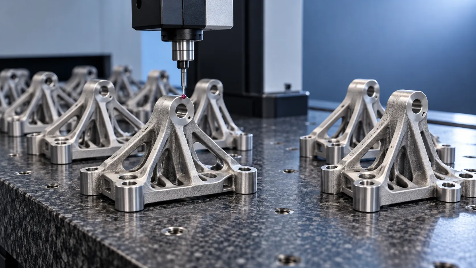
How to verify part consistency before choosing a 3D printing OEM
Choosing a 3D printing OEM? Learn how to verify part consistency with repeat-build trials, validated inspections, and traceability checks before committing to production.
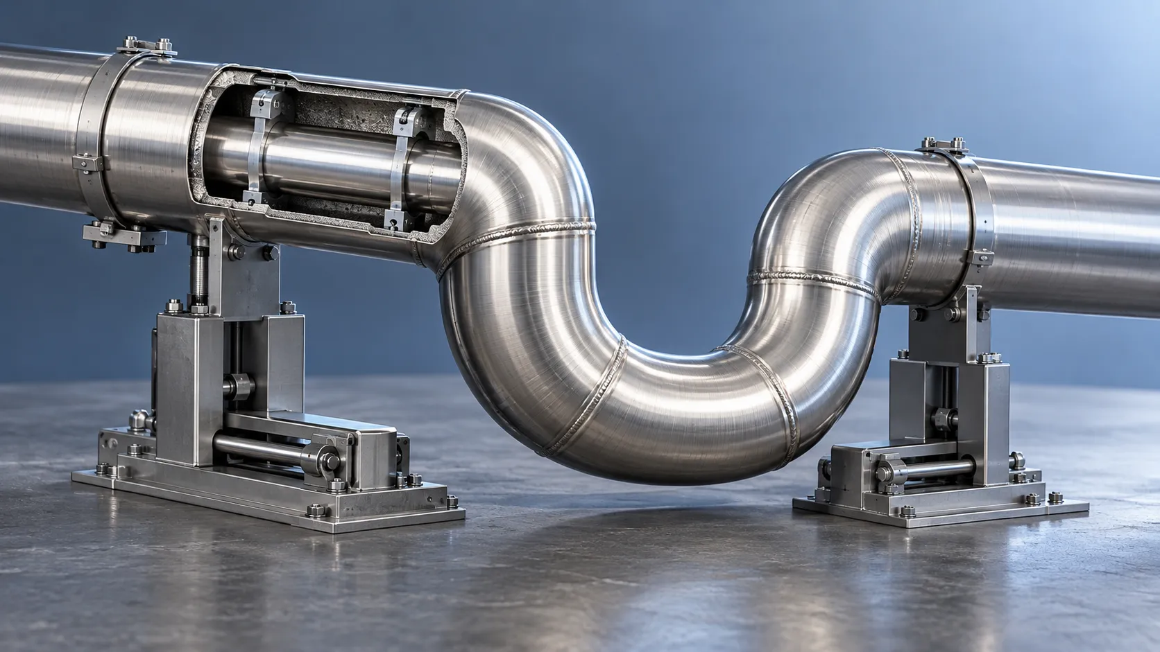
How does a rigid cryogenic transfer line handle thermal contraction?
Learn how a rigid cryogenic transfer line manages thermal contraction with bends, bellows, and guided supports. Discover key design checks for safe, reliable cryogenic performance.

How much does edge vision deployment cost beyond the hardware?
Understand edge vision deployment cost beyond hardware, from data and integration to security and support. Uncover hidden expenses and build a smarter lifecycle budget before you scale.
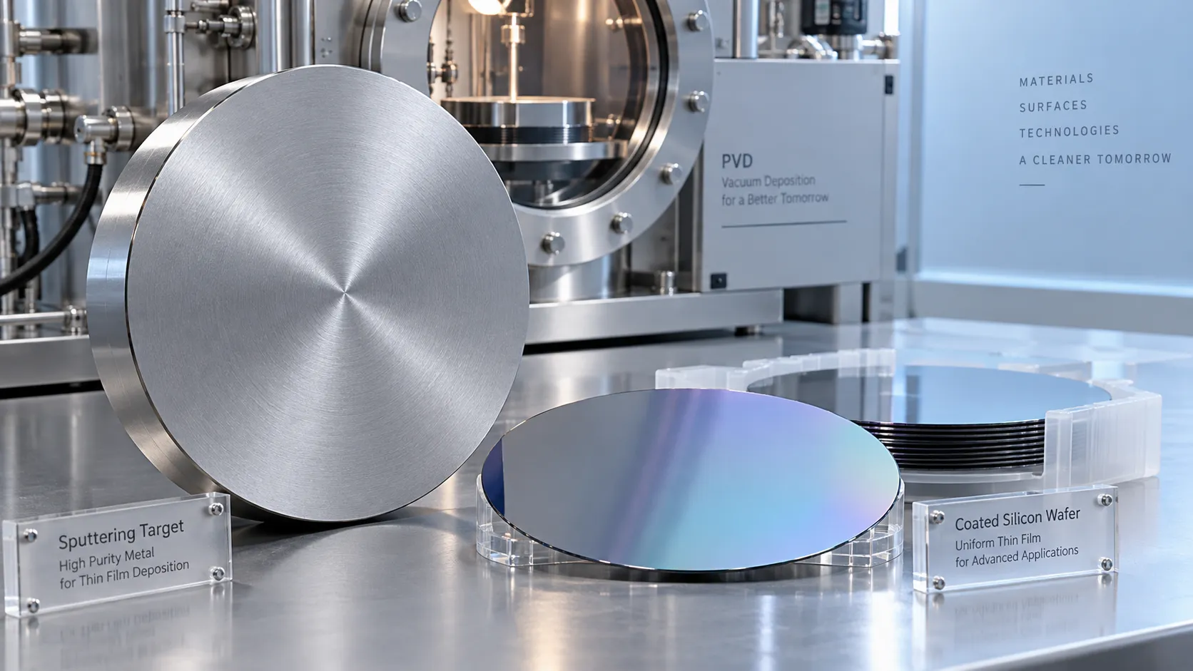
How does the purity of sputtering targets affect thin-film quality?
Discover how sputtering targets affect thin-film quality. Learn to assess purity, identify harmful impurities, and choose specifications that improve coating performance.

How high power laser cladding systems control substrate dilution
Discover how high power laser cladding systems control substrate dilution through beam shaping, material feed, and thermal management to deliver reliable bonds and coating performance.

How to check HS codes for customs compliance in international logistics
Strengthen international logistics customs compliance: learn how to verify HS codes, check official tariffs, and document classifications to reduce costly shipment delays.
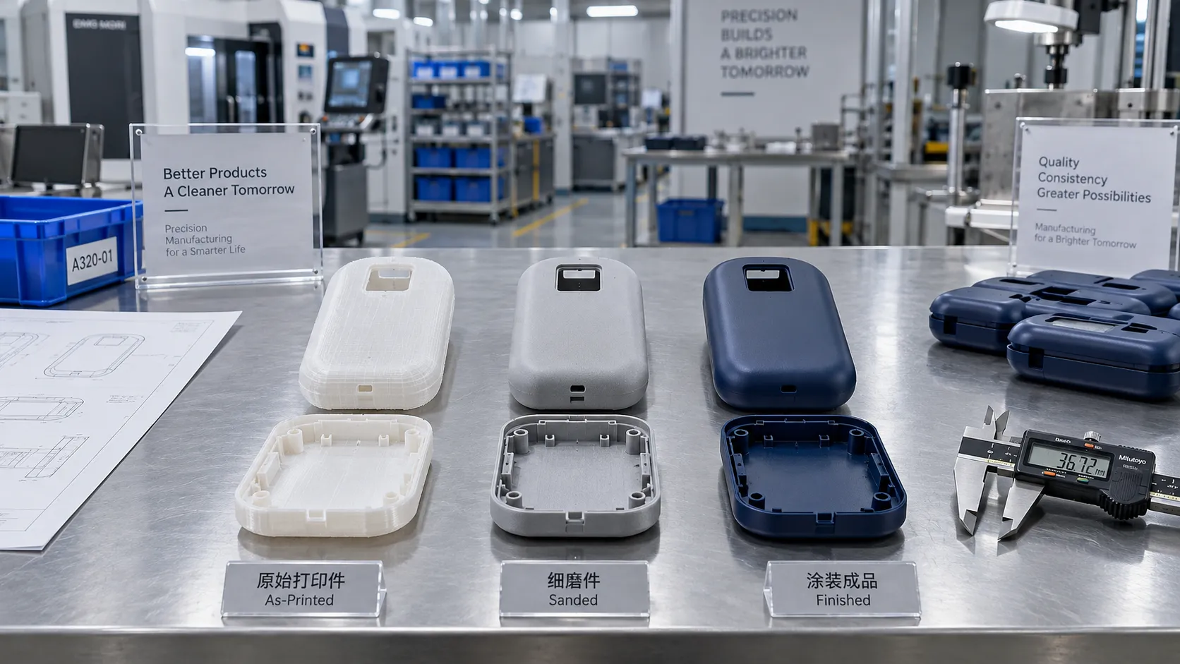
Choosing a 3D Printing Service for Consumer Products: Finish, Fit, and Cost
Compare 3d printing consumer good services by finish, fit, materials, and total cost. Learn how to choose a reliable supplier and avoid costly defects before ordering.
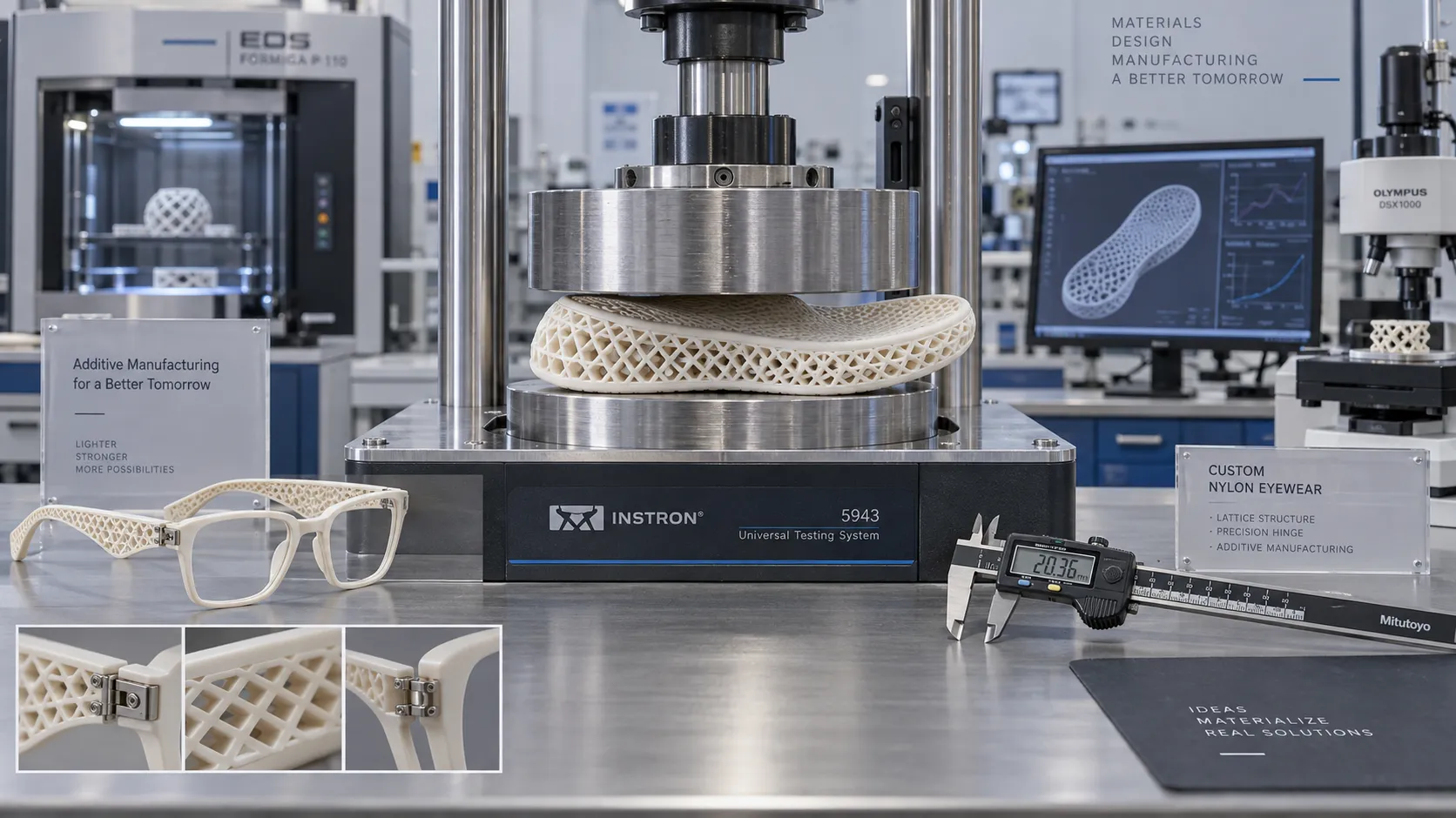
Which Consumer Goods Can Be 3D Printed, and What Are the Practical Limits?
Explore 3d printing consumer goods, from custom eyewear to replacement parts. Discover practical limits on materials, safety, and costs to make smarter production decisions.
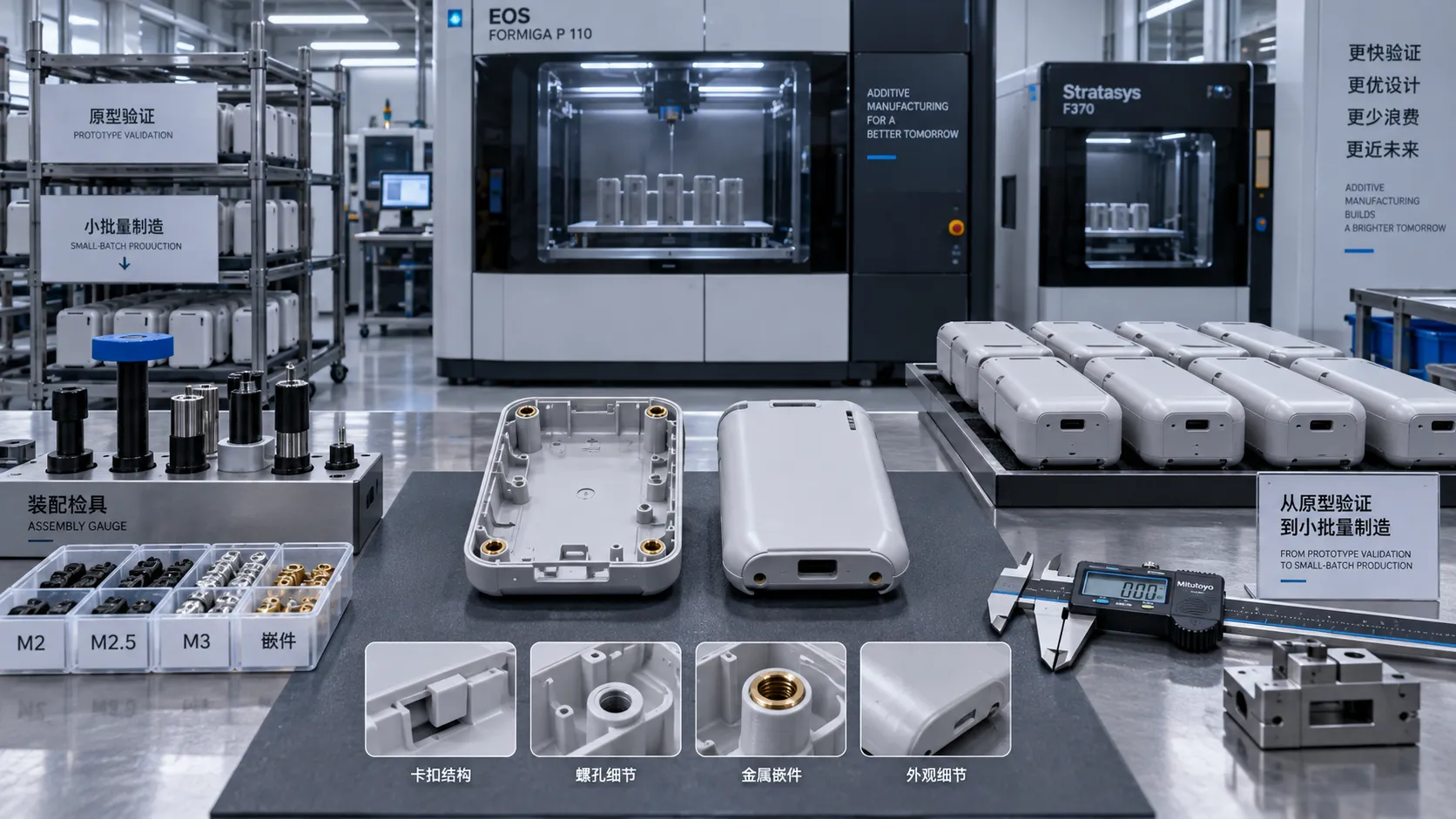
From Prototype to Small Batch: Applying 3D Printing to Consumer Goods
Explore 3d printing in consumer goods: learn how to move from prototype to small-batch production with practical guidance on materials, quality validation, and cost control.
Related News
- 00
0000-00
How to verify part consistency before choosing a 3D printing OEM - 00
0000-00
How does a rigid cryogenic transfer line handle thermal contraction? - 00
0000-00
How much does edge vision deployment cost beyond the hardware? - 00
0000-00
How does the purity of sputtering targets affect thin-film quality? - 00
0000-00
How high power laser cladding systems control substrate dilution
Dr. Elena Carbon
Weekly Insights
Stay ahead with our curated technology reports delivered every Monday.